Jeffrey's Log
Published on: May 06, 2012

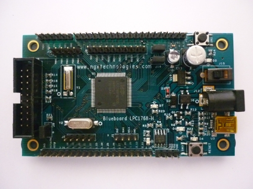
Above shown is a BlueBoard LPC1768 header board. I got this board from NGX technologies. This board contains an ARM cortex M3 based LPC1768 microcontroller from NXP (Philips). NGX technologies has similar ARM development boards which can be purchased from their webshop.
NGX technologies BlueBoard LPC1768 header board is of size 95mm x 55mm size. It has an power connector to connect DC power. The board can also be powered using its mini USB port. It also contains an LED and a switch(other than the rest switch) for basic operation. All the pins of the controller can be accessed through the header pin port. It also contains an JTAG port for debugging the ARM microcontroller. There is also an EEPROM chip to store information which is independent of the power.
The greatest advantage of this board is that it can be flashed using its USB port. There is no seperate flashing tool hardware or software needed. Just plug the board into the USB port and press a button sequence. The board will appear as an mass storage device(like our USB pen drives). The compiled bin just has to be pasted into the drive. Once the reset button is pressed, the new compiled software will start to work. More information can be found from here.
These type of header boards are really helpful when you want to prototype your designs. Its really hard for a newbie or even time consuming for an expert to design a PCB for the microcontroller and then start development. This board contains all the basic circuit to bring up the microcontroller and start development.
Some useful links
1) Google code page(contains complete source code and hardware design): http://code.google.com/p/blueboard-lpc1768/
2) Product page(Contains more information about this products and various tools): http://shop.ngxtechnologies.com/product_info.php?cPath=21&products_id=65
3) Documents form NXP for LPC1768: http://ics.nxp.com/support/documents/microcontrollers/?scope=LPC1768
Published on: November 18, 2011
This post contains mail written by me to the famous hacker Héctor Martín. The mail was regarding the basic steps in reverse engineering devices.
— MAIL BEGIN —
> 1) After opening a device, how do you understand which chip is the CPU ?
This is usually fairly obvious from the layout and the connectivity on the board. It really depends on the device, but it’s usually one of the larger chips, and may be connected to Flash memory, and/or to a quartz crystal. On larger devices it will have its own power supply, while on smaller ones the only telltale might be that it’s connected to most parts of the board. And of course, often you can just look up the part numbers and figure out what most chips are.
> 2) How are the firmwares extracted from the devices ? Is there a general principle ?
This depends heavily on the device. It can be as easy as connecting to a debug serial port and getting a text-based console into a bootloader that lets you dump the flash. Or it can be as hard as requiring a clock/power glitching setup in order to dump an internal mask ROM buried inside the CPU. Usually if the flash is external, you can remove it and dump it externally, or there might be a JTAG port through which you can read/write it. Microcontrollers with embedded flash usually have programming ports but the code is usually protected from readout; these are nearly impossible to dump unless you know of a specific vulnerability in the particular chip’s protection.
> 3) After getting a firmware dump how do you read it ?
If you know the CPU architecture in use, you run it through a disassembler and see if it makes sense. If you don’t know the architecture, you can try some educated guesses. After a while you learn to recognize some popular CPU architectures from a simple hex dump (e.g. ARM code sticks out like a sore thumb due to the condition code field, which means that every 32-bit word almost always starts with ‘E’). You can just use GNU binutils (objdump) to disassemble code (usually), but the IDA disassembler by Hex-Rays is quite popular in the reverse engineering community (albeit quite pricey). Sometimes the CPU architecture is unknown. I know some crazy people who can eventually make sense of an unknown binary and figure out what the opcodes mean, but I’m not one of them.
And sometimes if the firmware has very high entropy (it looks like “garbage” – no patterns, you learn to recognize this too) it usually means it’s either encrypted or compressed, so you might look to see whether you can find an offset after which there’s valid compressed data using a popular algorithm (zlib, LZMA, etc…). If it’s encrypted sometimes there are blockwise patterns (e.g. duplicated 16byte or 8byte blocks) that often mean it’s encrypted using a block cipher in ECB mode.
— MAIL END —
Published on: October 30, 2011
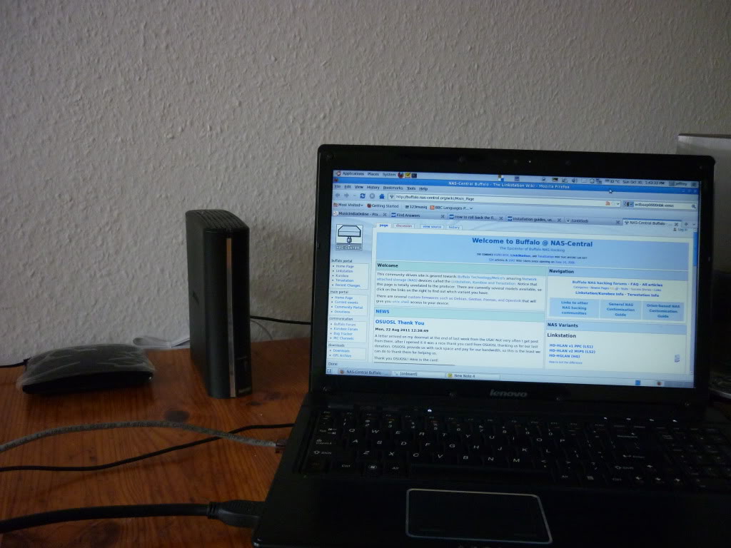
Below shown is my new LS-CH1.0TL LinkStation Live 1TB Buffalo-NAS purchased from MediaMarkt (Germany).

It supports one of my favourite feature – Its a hackable device! Flashing a new GNU/Linux firmware. Buffalo-NAS is based on GNU/Linux and also they provide its sourcecode in the downloads section webpage.
Also there is an dedicated hack portal for the Buffalo-NAS. Below is the link
Buffalo NAS-Central – http://buffalo.nas-central.org/wiki/Main_Page
I will post some hacks in my web log as I proceed.
Published on: May 26, 2011
Track every Watt(TEW) is one of the new Open Hardware based project which I am working on for the past few weeks. Track Every Watt is a pluggable device which can be used to measure power consumed by an electrical appliance. The device to be measured is connected to the TEW which has an LCD display which shows power consumed and also some additional information. TEW was inspired from Kill A Watt which is a device that can only measure devices with voltage rating 110V. TEW has a voltage rating of 230V and this is the reason why I started this project.

Track Every Watt can display additional information such as Voltage(V), Current(A), Watts(W), Volt-Amp(VA), Frequency(Hz), Power Factor(PF), Kilo Watt Hour(KWH), Time Elapsed. It uses an Analog Devices Energing Metering IC ADE7763. There is also an application note AN-564 for this IC.
Published on: March 12, 2011
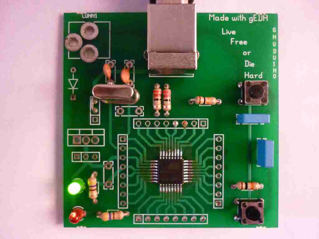
Two years before I had designed a mini development board for AT90USB162. There was a small mistake in that board. It didn’t have the 1MFD capacitor connected across the UCAP (PIN 27) and ground. Because of that the board was not detected while connected via USB. Last month I thought of repairing that board and do some USB projects. I ordered samples of ATMEGA32U2 from ATMEL. Thanks ATMEL for the samples.
Today I did a small hacking on the board. I added the capacitor as needed by USB. Now the board is working fine. There came the next problem. GCC-AVR version which I had, didn’t support ATMEGA32U2. Also for loading the hex into the controller, I used the dfu-programmer. Since I had installed it from the Ubuntu repository, dfu-programmer was of older version and it also didn’t support ATMEGA32U2.
After a few Google search, I found that if you compile for AT90USB162, the hex generated is supported by ATMEGA32U2. So I wrote the C code and compiled it for AT90USB162. Next task was to make the dfu-programmer to work. The only solution was to get the latest code and compile it. Below shown is the way to compile the dfu-programmer from source
$ mkdir dfu-programmer<br />
$ svn co https://dfu-programmer.svn.sourceforge.net/svnroot/dfu-programmer/trunk/ dfu-programmer<br />
$ cd dfu-programmer/dfu-programmer<br />
$ ./bootstrap.sh<br />
$ ./configure<br />
$ make
Once installed, flashing the controller is very easy. First we have to bring the controller into USB bootloader mode. For that first press and hold the RESET button. Then press and hold the HWB button. Now release the RESET button and then release the HWB button. This will bring the controller into USB bootloader mode. Now we can issue the following instructions to flash the controller.
$ dfu-programmer atmega32u2 erase<br />
$ dfu-programmer atmega32u2 flash blink.hex<br />
$ dfu-programmer atmega32u2 reset
This is an Open Hardware project and I will soon post the schematic and PCB layout once adding the missing capacitor in the old design. Below shown is the snap shot of the board.
